Applications

The versality and high throughput of the Atmospheric Dry Etching (ADE) technology makes it suitable for various industrial silicon etching and texturing applications. The ADE process unique features are : single side process, including wafer edges, very selective etch (SiOx, SiNx can be used as a mask/etch stop), fast etch rate, low temperature process, and works with any type of silicon.

TOPCON IBC ADVANCED TOPCON

> Poly-silicon removal for TOPCON solar cells

Tunnel oxide passivated contact (TOPCON) solar cells are seen as the next step to reach efficiencies higher than with the PERC process. TOPCON cells use the high surface passivation quality of deposited amorphous silicon for their rear side, on top of a thin tunneling oxide.

The state of the art deposition process however leads to parasitic deposition at the front of the wafer that needs to be removed, as well as around the edges of the wafer. It can result in parasitic absorption, shunting and irreversible hot-spot damage of the cell during module operation.

poly-Si-SEM-ADE.JPG
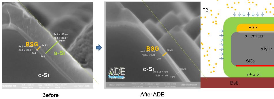
The single sided nature and high selectivity of the ADE process is particularly well suited to the removal of the poly-silicon from the front side of a wafer, during the manufacturing of a TOPCON solar cell. The a-Si can be etched either before of after annealing. The a-Si is removed from the top surface but critically, also from the wafer 's edges during the ADE process. The BSG under-layer is not etched, due to the high selectivity of the process, providing adequate protection to the cell's emitter, and more flexibility for the associated diffusion process. 

TOPCON Cells produced using ADE show very high parrallel resistance and low reverse current, avoiding any damage from hot-spot during module operation, and leading to higher module reliability.

"Atmospheric Pressure Dry Etching of Polysilicon Layers for Highly Reverse Bias‐Stable TOPCon Solar Cells", EUPVSEC Conference Proceedings, DOI: 10.1002/solr.202100481

Latest News

22/08/23 Selective etching for Advanced TOPCON & IBC

The ADE process meets the selective etching requirements of upcoming "Advanced TOPCON" solar cell architectures and IBC.


14/11/22 ADE for TOPCON cells - EUPVSEC 2022

In Milan's conference, Fraunhofer ISE presented its latest TOPCON cell developments, featuring ADE poly etching.


More news...


> Optimized Adhesion of Plated Silicon Solar Cell Contacts

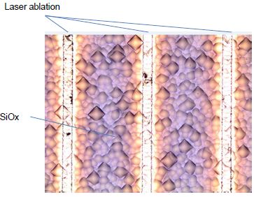
ADE is introduced as plating pre‐treatment to generate a beneficial nano‐roughness on the silicon substrate. The method is shown to improve the adhesion of solar cell contacts that are structured by local ablation of the passivation layer using ns‐pulsed lasers. Due to the high etch selectivity of the ADE process between silicon and silicon nitride, no additional etch mask is required to protect the passivation layer. In peel force tests on busbars, the average peel‐force raised from 0.3 to 2 N mm−1. In sheer‐test on finger contacts an increase of maximum sheer force and a decreasing length of the finger displacement are observed. 

>> Check the full paper:  LINK

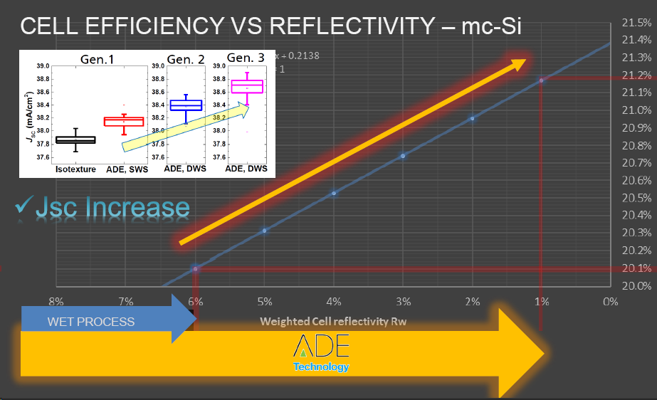
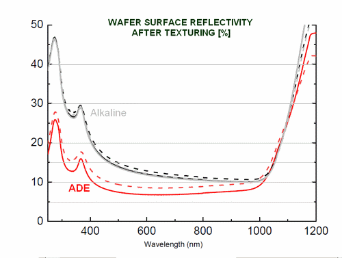
> Inverted pyramid texture for p-type mono wafers

In collaboration with Fraunhofer ISE, NinesPV are incorportating the ONYX texture ADE into p-type PERC cells. The process developed lead to lower reflectivities than the alkaline process by the formation of small random inverted pyramids. The reflectivity level can be controlled through the process.

APtexture.gif

Reflectivity_comparison_ADE_alkaline.gif

> Single side Emitter etch back/removal - edge isolation

The single-side and finely controllable ADE process is well suited for emitter etch back. Both front side and edges are targeted by the process. Complete removal and edge isolation is also possible.

wafersonbelt.JPG 

> FLUORINATION

Gas phase Fluorination of layers is also possible with the ADE platform. Its compatibility with roll to roll configuration makes it suitable for the continuous processing and dynamic fluorination of films. The typical reaction when applied to an organic compound is the substitution of hydrogen atoms by fluorine; direct fluorination involves a reaction of the C-H bond with the elemental fluorine. This is the most common method used for the fluorination of polymers.

ADE_roll_to_roll.JPG


> ONYX© SS TEXTURING FOR PERC

The texturing process of solar cells is the etching step with highest added value. It modifies the surface of the wafer in order to create a micro/nano scale surface texture that increases the amount of light absorbed into the silicon, and therefore increase the overall efficiency of the cell. Current wet processes have limited efficiency and require the deposition of additional anti-reflective layers on top of the cell.

mcSiEfficiencyVSReflectivity.png

Nines ONYX texturing process delivers surface textures with superior optical properties and reflectivity as low as 2%.The cells look darker providing best in class aesthetic for all type of wafers, including multi-crystalline.

The amount of silicon removed to achieve theses textures is minimal, leading to cost saving not only on etching consumables but also on silicon, i.e. the wafers could enter the factory thinner yet the finished cell would have the same thickness as for a wet process.

> ADE texture leads to PERC efficiency over 20%

NINES PV, Hanwha QCells and Fraunhofer ISE worked together to integrate the ADE dry texturing process into the well established Q.ANTUM PERC process. Using diamond wire (DW) cut mc-Si wafers, the ADE process resulted in an uplift compared to the standard reference due to the superior texturing leading to higher current. The results were presented at the 2017 EUPVSEC conference in Amsterdam: " Industrial Plasma-Less Dry Texturing Method for Diamond Wire Cut mc-Si Wafers -the universal ADE texturing process ".

>> Download the poster here

> Texturing diamond wire cut wafers

The ADE texturing process has been demonstrated with several types of crystalline wafers, inlcuding Cast wafers, Epitaxial layers, Diamond wire cut wafers, as well as amorphous deposited Si layers.

More specifically, for mc-Si diamond wire cut wafers, the ADE technology provides a high performance texturing solution for industrial customers willing to move from slurry cut to diamond wire cut wafers in order to avail of the full cost benefit that this technology brings (www.itrpv.net). The flexibility of the process allows a large variety of texture and reflectivity, down to “black-silicon” level, as would be achieved by a RIE vacuum based process.

> Laser damage etch

Laser contact opening through SiNx can lead to damage than needs to be etched. The ADE 's etch selectivity allows for direct etching, without interfering with the nitride/oxide layers, nor the back side of the wafer due to the single-side nature of the process.

laser_damage_etch.JPG

To access our published research papers on ResearchGate:  RSG